Product
XTPL® Delta Printing System
Explore our Open Prototyping Platform, delivering reliable, repeatable, and durable results for high performance materials. Easy to operate and maintain. Ideal tool for R&D in various microelectronics applications.
Our technology
Printing on the edge
- Edge interconnections printing
- High resolution traces, below 10 µm
- Possibility to print over the edge of glass, silicon and flexible foils
Redistribution layer prototyping
- All printed RDL structure
- Down to 1 μm / 1 μm L/S density
- Variable materials possible to use in one system, for example metallic nanoparticle paste and high viscous polyimide
Chip interconnection
- Reliable connection for flexible hybrid electronics and advanced IC packages
- High density interconnections on stacked chips
- Resolution <10 μm/10 μm L/S
- No satellite droplets and line width homogeneity to prevent electrical shorts
Get to know us
What makes us unique
- Feature size 1-10μm
- Fast & easy exchange of cartridges & nozzles
- Conductive and not conductive material support
- Printing on heterogeneous materials and 3D topographies
- Uniform & clean features geometries: no overflow or spills
- Only 0,1 ml of ink required to start printing
- Up to a 100% ink utilization
- High aspect ratios just after a single pass
- Matchless variety of printing materials: nanoinks, QD inks, dielectrics, photoresist, polymers
- Uninterrupted interconnections on highly complex topographies
- Ultra-high-resolution printing on practically any kind of substrate
- Ability to print high viscous materials along with small feature sizes
Example uses of Delta
Semiconductors
Displays
PCB
Biosensors


Suitable for various applications, such as:
- 3d interconnections
- Advanced IC packaging
- RDL prototyping
- TSV filling


DPS provides:
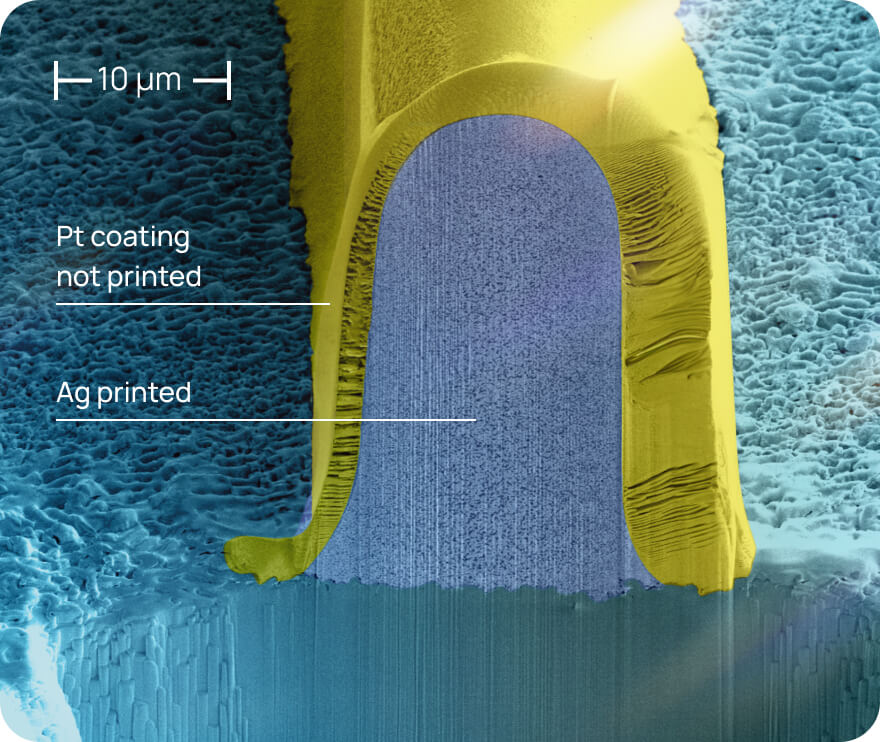
- High aspect ratios in a single pass benefit memory chips and MEMS
- No overflow or spills
- Reduced production costs
- Convenient cartridge and nozzle exchange
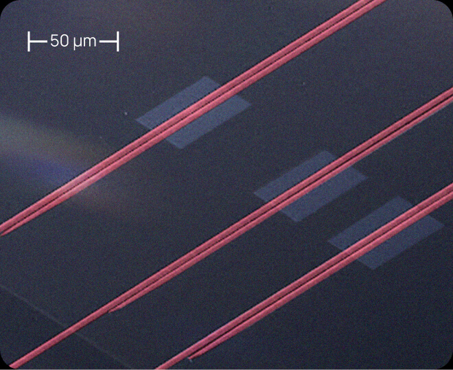
- High density interconnections down to 1 µm / 1 µm L/S


TFT arrays:
- Prototyping TFT and electrical circuit
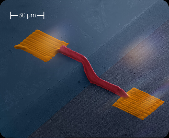
- Open defects repair
- No risk to damage discreate elements by eliminating electrical field
- Conductive structures down to 1µm

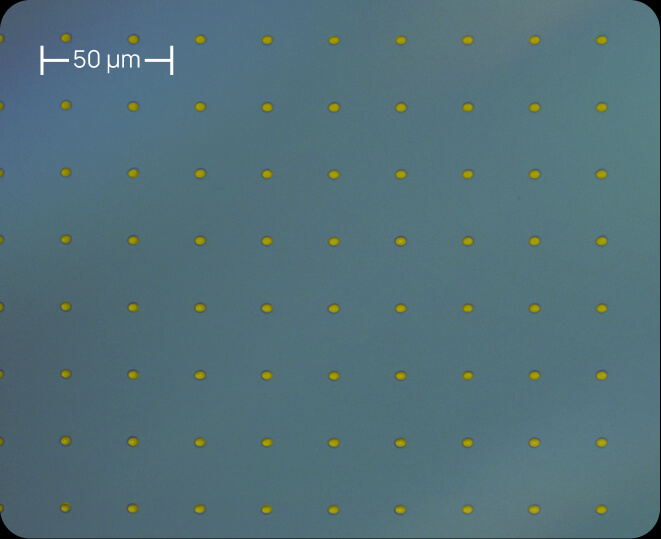
Quantum Dots Printing:
- DPS supports printing with Quantum Dots-based inks (QD inks)
- Its versatility is crucial for OLED and microLED
- With printed QD inks having a dimension of 3.5 µm width and below 300nm height, offers time and material savings and precision


Delta addresses specific challenges in the prototyping and fabrication of modern PCBs:
- Ultra-high resolution printing and feature sizes of 1‑10 μm tackles the design complexity and enables the creation of specific PCB structures
- Versatility allows for the integration of diverse materials, both conductive and non-conductive, while maintaining high aspect ratios in a single pass


We ensure:
- Printing on 3D topographies feature uniformity
- The reliability and performance of the PCBs
- A comprehensive solution for modern PCB manufacturing


Our innovative biosensor solution:
- High performance
- Size reduction
- Cost-effective fabrication methods
- Groundbreaking for rapid biosensor prototyping
- Enables biosensing patterns on flexible substrates, crucial for wearable sensors

Delta system ensures:
- Uniform, clean features without spills crucial for intricate biosensor designs
- Maintaining reliability and accuracy
Achieve unparalleled accuracy
Prototype microelectronic devices with exceptional precision using our XTPL® Delta Printing System and high-viscosity conductive inks.
Partners’ testimonials
Prof. Norbert Fruehauf
Director of IGM at University of Stuttgart
The XTPL’s ability to directly deposit (in a mask-less approach) electrically conductive structures in the minimum feature size range of 1.5 – 10 micrometers is unique. In my view the XTPL’s ultra-precise deposition technology offers truly unique properties, which are an excellent fit to the future needs in the field of printable high-resolution and foldable OLED displays.
Prof. Ravinder Dahiya
The Leader of the BEST research group at the University of Glasgow
Our research revolves around the development of high-performance printed electronics and sensing systems on large area flexible substrates. We used these printed systems to develop flexible electronic skin (eSkin) and explore its application in healthcare, wearable systems and robotics. In our projects we also use micro/nanofabrication tools and align them with processing on flexible substrates. We decided to purchase the Delta Printing System for our labs, after performing initial tests with the team at XTPL over the last several months. This appears to be a great enabling tools and we are looking forward to including it in our daily research work.
Do Soon Jung
Vice President at HB Technology
Our relationship with the XTPL team has successfully continued for 24 months now. In that time, we have deeply evaluated different printing technologies available worldwide for some of the most challenging use-cases in ultra-high resolution next generation displays. In our collaboration, the XTPL team demonstrated that their technology has a unique technological solution and a very good potential to enable manufacturing of the next generation flat panel displays. Putting the XTPL device to use for validation of the XTPL technology at the R&D level will help us to strengthen the collaboration and accelerate the joint introduction of XTPL technological solutions to our end customers, who are the leading global manufacturers of FPDs. We are looking forward to growing our relationship and collaboration with the XTPL team for the future.
Prof. dr Emil List-Kratochvil
Head of the Hybrid Devices group and expert in organic semiconductors and printed semiconductor devices., Humboldt University of Berlin
We became very much interested in the UPD method developed by the XTPL team. We first learned about it and the Delta Printing System at the ISFOE conference series in 2021. After we had the opportunity to find out about the capabilities of the method, we decided that the device would be a great tool for our scientists who are working on new technologies for sensor, photovoltaic and optoelectronic solutions. We are not going to stop at the academic research phase: moving forward, we’re planning to implement the results in real-life applications at our industrial partners who have been cooperating with our institute for a long time.
Prof. Fabrizio Torricelli
University of Brescia
One of the focus areas for our research is the development of assistive technologies for the production of a modern class of biosensors, which are sought after by global industrial clients and which must satisfy their current requirements, including in terms of environmental protection. Another aspect is the ability to micro -fabricate – or build micrometric devices and components. Microfabrication of bioelectronic devices for detecting a single molecule requires the capability of applying ultra-thin conductive structures with a width and pitch below 1 micrometer, as well as with an appropriate viscosity index. Until now, our University did not have a proper system for this purpose – no such solution was available on a global scale.
Clients’ publications
FLEXIBLE QUANTUM-DOT LIGHT-EMITTING DIODES USING EMBEDDED SILVER MESH TRANSPARENT ELECTRODES MANUFACTURED BY AN ULTRAPRECISE DEPOSITION METHOD
Authors: Łukasz Witczak, Maciej Chrzanowski, Piotr Sitarek, Mateusz Łysień, and Artur Podhorodecki
Check moreULTRAPRECISE PRINTING OF D-BAND TRANSMISSION LINES
Authors: Martin Roemhild, Georg Gramlich, Holger Baur, Thomas Zwick, Norbert Fruehauf
Check moreHIGH FREQUENCY SOLUTION-PROCESSED ORGANIC FIELD-EFFECT TRANSISTORS WITH HIGH-RESOLUTION PRINTED SHORT CHANNELS
Authors: Tommaso Losi, Łukasz Witczak, Mateusz Łysien, Pietro Rossi, Paola Moretti, Chiara Bertarelli, Virgilio Mattoli, and Mario Caironi
Check more3D PATTERNING – AN EXTENDED TOOLBOX FOR MICRO-ELECTRO-MECHANICAL SYSTEMS
Authors: H.K. Trieu, L. Rennpferdt, and S. Bohne
Check moreALL-PRINTED ZNO NANOWIRE BASED HIGH PERFORMANCE FLEXIBLE ULTRAVIOLET PHOTODETECTORS
Authors: Sihang Ma, Abhishek Singh Dahiya, Adamos Christou, Luca De Pamphilis, Ravinder Dahiya
Check more
HIGH-RESOLUTION DEPOSITION OF CONDUCTIVE AND INSULATING MATERIALS AT MICROMETER SCALE ON COMPLEX SUBSTRATES
Authors: Mateusz Łysień, Łukasz Witczak, Aneta Wiatrowska, Karolina Fiączyk, Jolanta Gadzalińska, Ludovic Schneider, Wiesław Stręk, Marcin Karpiński, Łukasz Kosior, Filip Granek, Piotr Kowalczewski
Check moreQUANTUM DOTS BASED TRANSPARENT LIGHT EMITTING DIODES
Authors: Maciej Chrzanowski, Łukasz Witczak, Artur Podhorodecki
Check moreULTRA-THIN CHIPS WITH PRINTED INTERCONNECTS ON FLEXIBLE FOILS
Authors: Sihang Ma, Yogeenth Kumaresan, Abhishek Singh Dahiya, Ravinder Dahiya
Check morePRINTING OF NANO- TO CHIP-SCALE STRUCTURES FOR FLEXIBLE HYBRID ELECTRONICS
Authors: Adamos Christou, Sihang Ma, Ayoub Zumeit, Abhishek Singh Dahiya, Ravinder Dahiya
Check moreHIGH-RESOLUTION PRINTING OF REDISTRIBUTION LAYERS FOR FAN-OUT WAFER-LEVEL PACKAGING BY USING ULTRA-PRECISE MICRO-DEPOSITION TECHNOLOGY
Authors: Ali Roshanghias, Marc Dreissigacker, Iwona Gradzka-Kurzaj, Alfred Binder, Martin Schneider Ramelow, Łukasz Witczak, Tanja Braun
Check moreALL-PRINTED ZNO NANOWIRE BASED HIGH PERFORMANCE PHOTODETECTORS
Authors: Sihang Ma, Abhishek Singh Dahiya, Adamos Christou, Ravinder Dahiya
Check moreDIRECT WRITE 3D-PRINTED INTERCONNECTS FOR HETEROGENOUS INTEGRATION OF ULTRA THIN CHIPS
Authors: Sihang Ma, Abhishek Singh Dahiya, Ravinder Dahiya
Check morePRINTING OF MICROMETER-SIZE FEATURES ON COMPLEX SUBSTRATES FOR SYSTEM INTEGRATION
Authors: Aneta Wiatrowska, Karolina Fiączyk, Piotr Kowalczewski, Mateusz Łysień, Łukasz Witczak, Jolanta Gadzalińska, Iwona Grądzka-Kurzaj, Ludovic Schneider, Łukasz Kosior, Filip Granek
Check more
Take a moment to explore our brochure.
Learn how the first fully additive technology for printing lines with single-micrometer width works.
Download PDFContact us
- We will introduce our product
- We will explain how you can utilize it in your work
- We will address your questions and provide guidance
Talk to us:

Our Linkedin

EXPERIMENT RESULT
XTPL & QustomDot are pioneering flexible microLED displays in the EU-funded BAMBAM Horizon Europe project.

RDL PROTOTYPING
Accelerate Redistribution Layer (RDL) Prototyping with the XTPL #DeltaPrintingSystem!

PRINT ON HUMAN HAIR
Ease of Use Meets Advanced Technology: The XTPL Delta Printing System!